The Last Barrier To Ultra-Miniaturized Electronics Is Broken, Thanks To A New Type Of Inductor

One of the three basic circuit elements just got a lot smaller for the very first time, in what promises to be a trillion-dollar breakthrough.
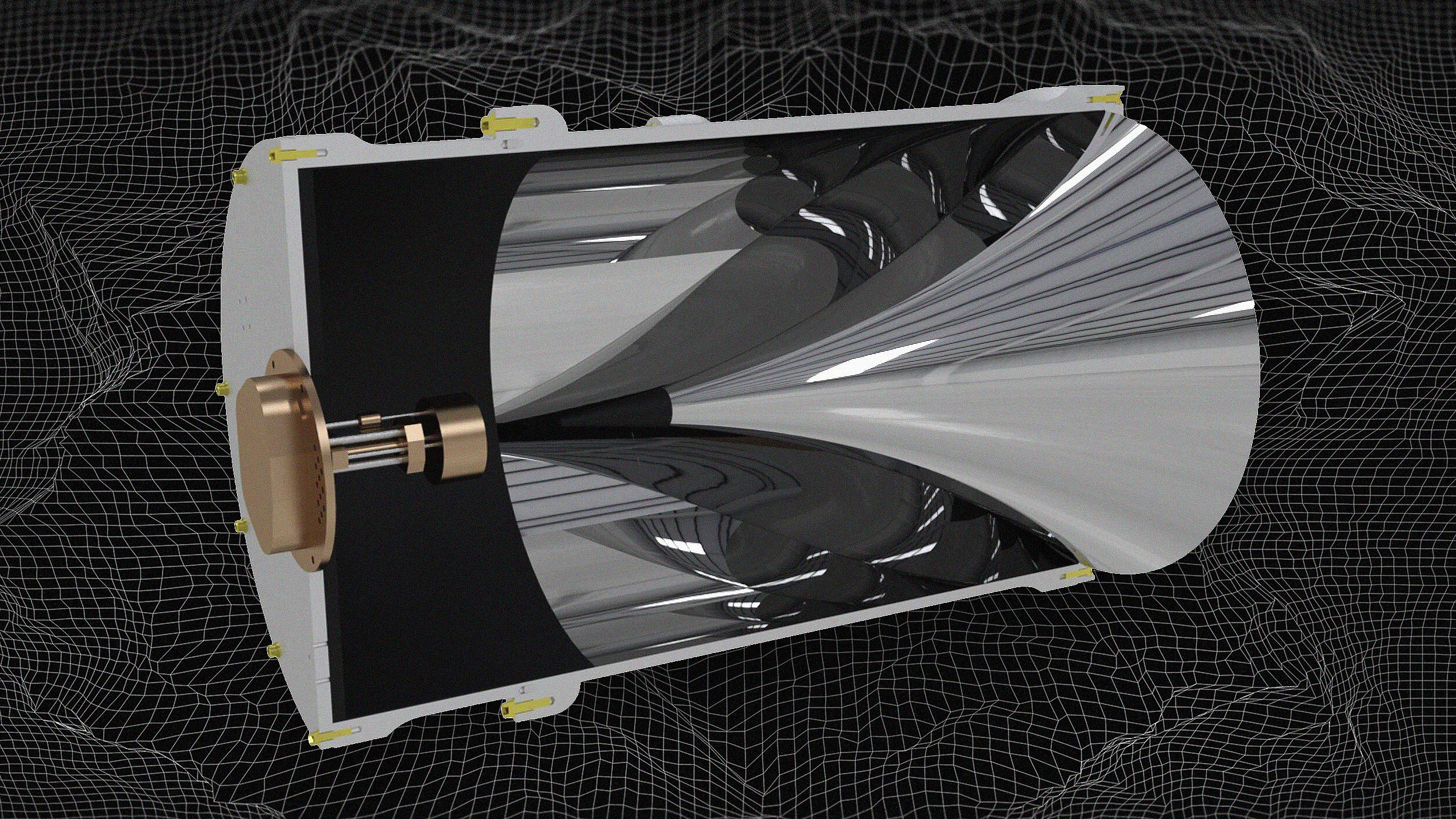
In the race for ever-improving technology, there are two related technical capabilities that drive our world forward: speed and size. These are related, as the smaller a device is, the less distance the electrical signal driving your device has to travel. As we’ve been able to cut silicon thinner, print circuit elements smaller, and develop increasingly miniaturized transistors, gains in computing speed-and-power and decreases in device size have gone hand-in-hand. But at the same time these advances have comes in leaps and bounds, one fundamental circuit element — the inductor — has had its design remain exactly the same. Found in everything from televisions to laptops to smartphones to wireless chargers, radios, and transformers, it’s one of the most indispensable electronic components in existence.
Since their 1831 invention by Michael Faraday, their design has remained basically unchanged. Until last month, that is, when a UC Santa Barbara team led by Kaustav Banerjee demonstrated a fundamentally new type of inductor. Without the limitations of the original inductor design, it should allow a new breakthrough in miniaturization and speed, potentially paving the way for a more connected world.
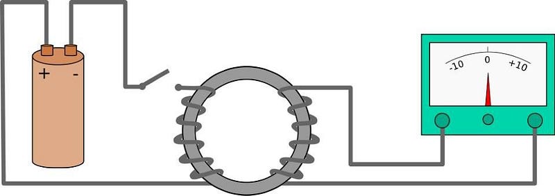
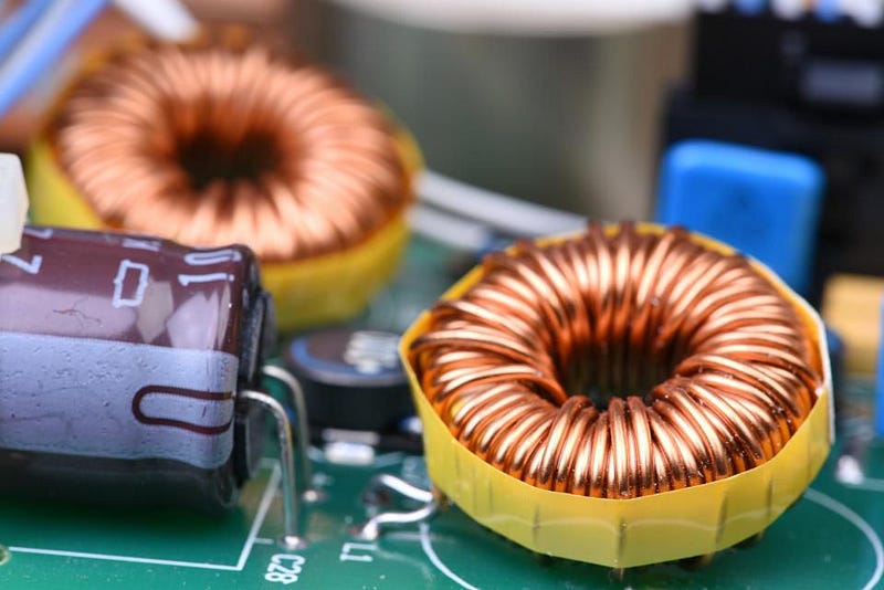
The classic way inductors work is one of the simplest designs possible: a simple coil of wire. When you pass a current through a loop or coil of wire, it creates a magnetic field through the center. But according to Faraday’s law of induction, that changing magnetic field then induces a current in the next loop, a current which opposes the one you’re trying to create. If you create a greater coil density, or (even better) put a core of magnetizable material inside the inductor, you can greatly increase the inductance of your device. This results in inductors which are very effective, but also which are required to be physically quite large. Despite all the advances we’ve made, the fundamental limitation of this design style means there’s been a limit to how small an inductor can get.
The applications, however, are tremendous. Along with capacitors and resistors, inductors are one of the three passive elements that are the foundations of all electronics. Create an electric current of the right magnitude and frequency, and you’ll build an induction motor. Pass the magnetic core in-and-out through the coil, and you’ll generate electricity from a mechanical motion. Send both AC and DC currents down your circuit, and the inductor will block AC while allowing DC to pass through. They can separate signals of different frequencies, and when you use a capacitor along with an inductor, you can make a tuned circuit, of paramount importance in television and radio receivers.
But while resistors have been miniaturized with, for example, the development of the surface mount resistor, and capacitors have given way to supercapacitor materials that approach the theoretical limit, the basic design of inductors has remained the same throughout the centuries. Despite being invented way back in 1831, nothing about their basic design has changed in nearly 200 years. They function on the principle of magnetic inductance, where a current, a coil of wire, and a core of magnetizable material are used in tandem.
But there is another approach, in theory, that inductors can take. There’s also a phenomenon known as kinetic inductance, where instead of a changing magnetic field inducing an opposing current as in magnetic inductance, it’s the inertia of the particles that carry the electric current themselves — such as electrons — that oppose a change in their motion.
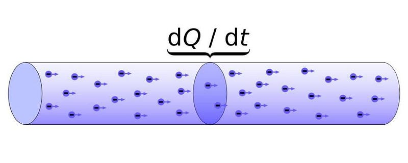
If you envision an electric current as a series of charge carriers (like electrons) all moving steadily, in a row, and at a constant speed, you can imagine what it would take to change that current: an additional force of some type. Each of those particles would need a force to act on them, causing them to accelerate or decelerate. The same principle that creates Newton’s most famous law of motion, F = ma, tells us that if we want to change the motions of these charged particles, we need to exert a force on them. In this equation, it’s their masses, or the m in the equation, that resists that change in motion. That’s where kinetic inductance comes from. Functionally, it’s indistinguishable from magnetic inductance, it’s just that kinetic inductance has only ever been practically large under extreme conditions: either in superconductors or in extremely high-frequency circuits.
In conventional metallic conductors, kinetic inductance is negligible, and so it’s never been applied in conventional circuits before. But if it could be applied, it would be a revolutionary advance for miniaturization, since unlike magnetic inductance, its value doesn’t depend on the inductor’s surface area. With that fundamental limitation removed, it could be possible to create a kinetic inductor that’s far smaller than any magnetic inductor we’ve ever made. And if we can engineer that advance, perhaps we can take the next great leap forward in miniaturization.

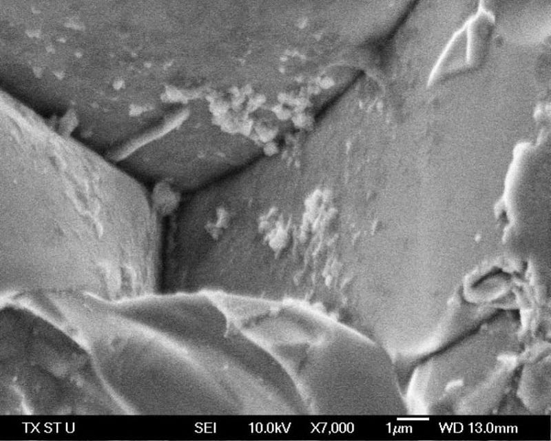
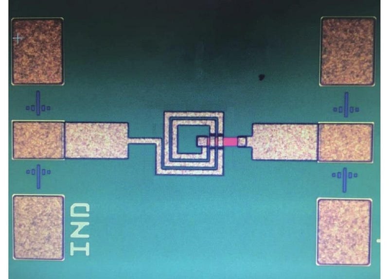
That’s where the work of Banerjee’s Nanoelectronics Research Lab and their collaborators comes in. By exploiting the phenomenon of kinetic inductance, they were able to, for the first time, demonstrate the effectiveness a fundamentally different kind of inductor that didn’t rely on Faraday’s magnetic inductance. Instead of using conventional metal inductors, they used graphene — carbon bonded together into an ultra-hard, highly-conductive configuration that also has a large kinetic inductance — to make the highest inductance-density material ever created. In a paper last month published in Nature Electronics, the group demonstrated that if you inserted bromine atoms between various layers of graphene, in a process known as intercalation, you could finally create a material where the kinetic inductance exceeded the theoretical limit of a traditional Faraday inductor.
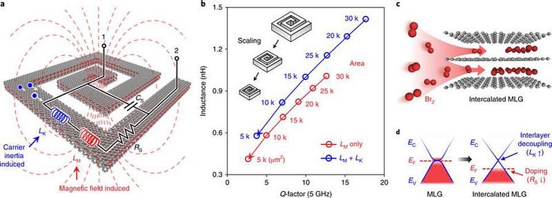
Already achieving 50% greater inductance for its size, in a scalable way that should allow material scientists to miniaturize this type of device even further. If you can make the intercalation process more efficient, which is exactly what the team is now working on, you should be able to increase the inductance density even further. According to Banerjee,
We essentially engineered a new nanomaterial to bring forward the previously ‘hidden physics’ of kinetic inductance at room temperature and in a range of operating frequencies targeted for next-generation wireless communications.
With connected devices and the Internet of Things poised to become a multi-trillion dollar enterprise by the mid-2020s, this new type of inductor could be exactly the kind of revolution the burgeoning industry has been hoping for. Next-generation communications, energy storage, and sensing technologies could be smaller, lighter, and faster than ever. And thanks to this great leap in nanomaterials, we might finally be able to go beyond the technology that Faraday brought to our world nearly 200 years ago.
Ethan Siegel is the author of Beyond the Galaxy and Treknology. You can pre-order his third book, currently in development: the Encyclopaedia Cosmologica.