Physicists solve a 140-year-old mystery
Credit: IBM
- Researchers discover a method of extracting previously unavailable information from superconductors.
- The study builds on a 19th-century discovery by physicist Edward Hall.
- The research promises to lead to a new generation of semiconductor materials and devices.
New research, led by IBM, made a breakthrough in resolving a mystery that has baffled physicists for 140 years. It promises to lead to a new generation of semiconductor materials and devices that use them.
The invention of semiconductors was instrumental in bringing on our digital age. You can find these electricity-carrying substances in your smartphone and computer. An improvement in this field could have major ramifications for future gadgetry.
In 1879, the American physicist Edward Hall discovered the Hall effect, showing that you can measure how electricity in a conductor flows. He found that because a magnetic field deflects the movement of electronic charges in a conductor, you can measure the amount of that deflection. This number will describe the voltage perpendicular (or transverse) to the flow of charge.
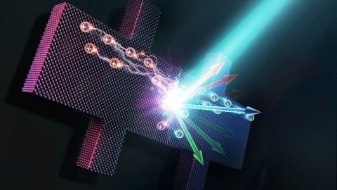
Modern researchers recognized, that you can also make Hall effect measurements using light in so-called photo-Hall experiments that generate multiple carriers (or electron-hole pairs) in superconductors. Unfortunately, while the Hall voltage provides crucial information about these charge carriers in a semiconductor, it is limited to the properties of the dominant (or majority) charge carrier, explain contributing authors Oki Gunawan and Doug Bishop in a post on IBM’s research blog.
Figuring out the information about both the majority and minority charge carriers, which impact changes in conductivity, would be key to advancing applications utilizing light, including optoelectronic devices like solar cells, LEDs, and lasers as well as artificial intelligence tech.
Now a new formula and technique for getting both the majority and minority carrier information was developed by researchers from KAIST (Korea Advanced Institute of Science and Technology), KRICT (Korea Research Institute of Chemical Technology), Duke University, and IBM.
The method, dubbed Carrier-Resolved Photo Hall (CRPH), measurement, can simultaneously extract information about the majority and minority carriers like density and mobility, carrier lifetimes and lengths of diffusion. In fact, compared to the three parameters of measurement traditionally derived by engaging the Hall effect, the novel technique can get up to seven parameters of information.

Credit: Gunawan/Nature magazine
The approach also takes advantage of a tool developed by IBM called the parallel dipole line (PDL) trap, which generates an oscillating magnetic field. It works as an ideal system for photo-Hall experiments because of the large amount of space it allocates for sample illumination.
If you’d like to dive more into the subject, check out the new study published in Nature magazine.

